OPTICS DLC CLARUS
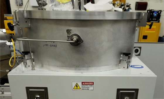
When you need high durable DLC then OPTICS DLC CLARUS by Thin Film Service is a fully automated PECVD platform for DLC, Infrared anti-reflective coating and other PECVD applications with excellent chemical and wear resistance, passing MIL-F-48616 / MIL-C-48497C.
OPTICD DLC CLARUS has several unique features,
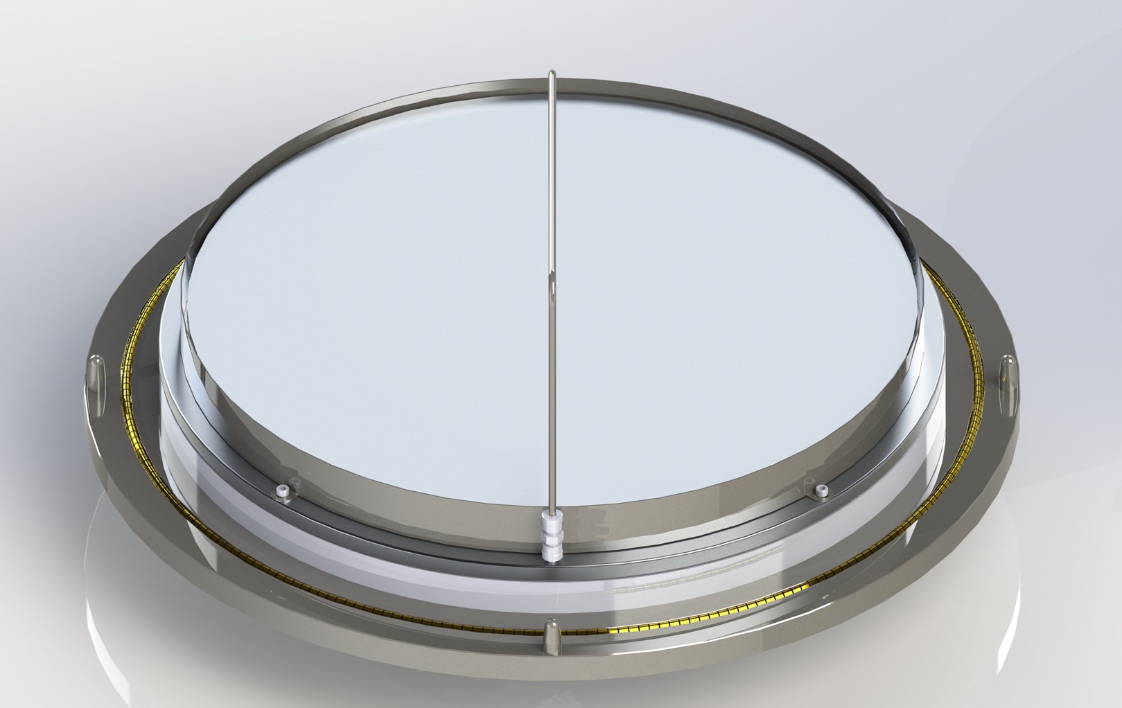
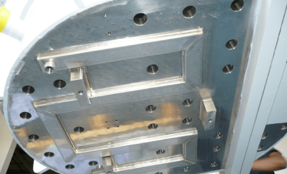
Firstly, with Ø585mm diameter, the capacity is amongst the largest in the field and can hold substrates with almost any shape or geometry, up to a diameter of 550mm with a height of 70 to 80mm for single substrates, or produce vast throughput of smaller parts with a batch time of ~1h.
Secondly, The deposition temperature is cold (<60°C), this limits exposure to hot substrates but it also reduces stress and flaking of the coating when coating, seed layer and substrate have a thermal expansion mismatch.
Thirdly, OPTICS DLC CLARUS has a self clean feature so each batch produces consistently uniform films that are up to several microns thick on a variety of substrates with little to no run-to-run variation.
Fourthly, and because the tool is 100% symmetrical in its design and build, it offers excellent uniformity! Where competing DLC tools have the pump port and the plasma charge port offset, OPTICS DLC CLARUS has both centered.
Fifthly, and the most important to achieve high yield is the excellent layer control. Twenty years of DLC deposition experience onto high value semiconductor pedestals has taught (and forced) us to design our own layer control software and PID's. This guarantees each step of the process transition is executed in a smooth, controlled and effective way so each product run is copy-exact.
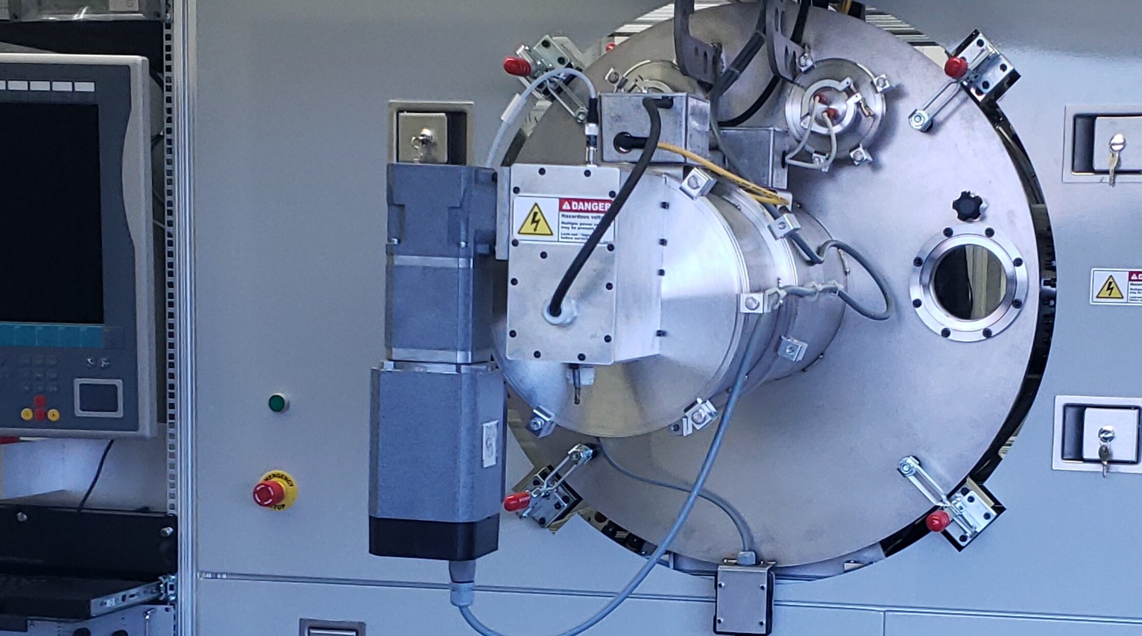
Lastly, with a footprint of 1500mm [59"] x 1200mm [48"] it takes up little space. There is no 19" rack that needs to be installed, no cables running over the floor. All components are integrated within a single chassis keeping the floor and work environment clean of dust which contributes to yield improvements. Dust = nodules. The entire tool rolls on castors so without our help, it can be moved around if you need to do so.
Examples of substrate materials include:
Si, Ge, II-VI compounds, optical glasses, chalcogenides, sapphire, metals, and plastics.
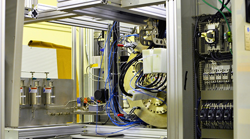
OMNIA SEMICONDUCTOR
The OMNIA pedestal-wafer contact surface performer offers a comprehensive, reliable solution to increase wafer to pedestal interface performance by reducing particle formation, improve electrical properties, thermal conductivity, corrosion protection and wear resistance which extends your pedestal lifetime by 4x when compared with TiN alternatives.
Versatile and customizable, the system can be configured to accommodate 200mm to 450mm ESC's addressing the needs for high current ION pedestals and PVD Minimum contact area (MCA) electrostatic chucks. Both Coulomb and Johnsen Rahbek (JR) processes are supported.
A sophisticated graphic user interface combined to a fully automated system allows for nightly ghost runs with a single push of a button. The proprietary TOPS GUI interface delivers flexibility and ease of use with attractive graphics and full data logging capabilities.
How can we help? Click here to let us know how we can be of service. Thanks for visiting!
OPTIKA+DLC
Thin Film Service's OPTIKA+ DLC is our most advanced Optical DLC coater systems that deliver ultra-dense DLC in a low pressure, clean environment, eliminating contaminants and pinholes while producing MWIR, LWIR wear- and corrosion resistant layers with rapid pump down times. Supporting a variety of substrates and substrate holders, including planetary systems to increase uniformity. Its vertical orientation guarantees a pinhole free film for both PVD layers, included but not limited to Ge, Yttrium and Si and PECVD DLC layers by eliminating "landing zones" for seeds that are pinhole initiation sites.
Suitable substrates are Ge, Si, ZnS, ZnSe and chalcogenide.
How can we help? Click here to let us know how we can be of service. Thanks for visiting!
OMNIA iDLNTM SEMICONDUCTOR
The OMNIA pedestal-wafer contact surface performer offers a comprehensive, reliable solution to increase wafer to pedestal interface performance by reducing particle formation, improve electrical properties, thermal conductivity, corrosion protection and wear resistance which extends your pedestal lifetime by 4x when compared with TiN alternatives.
Versatile and customizable, the system can be configured to accommodate 200mm to 450mm ESC's addressing the needs for high current ION pedestals and PVD Minimum contact angle (MCA) electrostatic chucks. Both Coulomb and Johnsen Rahbek (JR) processes are supported.
A sophisticated graphic user interface combined to a fully automated system allows for nightly ghost runs with a single push of a button. The proprietary TOPS GUI interface delivers flexibility and ease of use with attractive graphics and full data logging capabilities.
How can we help? Click here to let us know how we can be of service. Thanks for visiting!
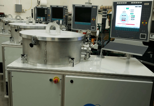
INTUOR - R&D and Universities
The INTUOR R&D System benefits from the same platform and our house developed TOPS GUI. This includes comprehensive datalogging capabilities, process visualization and a sophisticated graphic user interface. Developed in collaboration with customers, the TOPS program delivers flexibility and ease of use.
INTUOR can be operated in manual mode or fully automated whilst logging over one thousand data points. Reports can be created using the proprietary editor of through export in Excel at no additional cost.
Parameters can be adjusted up or down using extreme precision sloping (Ex. +/- 0.0024 sccm/sec).
System can be equipped with RF, MF, Pulsed DC, straight DC or HIPIMS and comprise of several MFC and evaporators to cover a wide range of CVD and PVD applications. INTUOR also has the unique ability to co-deposit PVD and PECVD films simultaneously
Versatile and customizable, the system can be configured to accommodate up to twelve cathodes in confocal or non-confocal settings and offers vertical adjustment, achieving a uniform, durable coating.
Our carousels are available with secondary and tertiary rotation and z-adjust, resulting in highly uniform and durable hard coatings. Configurable to almost any deposition methodology, Aphrodite sputtering systems enhance uniformity, increase production and minimize downtime.
How can we help? Click here to let us know how we can be of service. Thanks for visiting!
MULTUS PECVD/PVD iDLN
The MULTUS PECVD/PVD system offers an unparalleled innovative design and geometry therefore creating unique pinhole free films.
Firstly, the vertically oriented substrate eliminates nodule growth on both substrate and magnetron, therefore creating pinhole free films.
Secondly, the unique ability to simultaneously deposit plasma assisted hydrogenated DLC/DLN films whilst doping with PVD metallic and dielectric films allows for the development of blended, doped or a combination of both. a-C:H:Si:O:F:ME (X) has been developed and is patent pending. This film has shown to withstand over 800°C continuously in atmosphere.
Thirdly, The low temperature deposition (<60°C without cooling) allows production onto flexible and soft substrates.
Fourthly, and not least importantly, the system has a front and back door, which is perfect for cleanroom integration. Shield cleaning or exchange happens on the dirty side of the coater.
MULTUS offers the advantage of highly uniform and conformal coatings, producing superior results on even three-dimensional and detailed (intricately shaped) substrates. Optional customizable features such as feedthroughs, planetary systems and chamber configurations ensure optimal processing speed and uniform, corrosion-resistant coating, reducing production time and expense.
ABLUO Etch/Asher
The ABLUO etch/asher system has the fastest DLC removal rate when compared to our competitors, plus unlike other DLC ashers the ABLUO also has the ability to remove Silicon based DLC's.
ABLUO benefits from the same GUI and automation typical for our platform

Features
Don’t see the solution to your unique operational challenge here? Please ask! Our library of solutions and experience extends beyond what is on website and is constantly evolving.